Language: 

Michael Dytskov
Expert in the field of power supplies and power electronics.
Develop and manufacture various radio-electronic devices.
Some of my developments are represented on this page. You may also be interested in co-operation with me.
Simple switching power supply 5V, 4A
Power source is a single-pulse flyback voltage converter with self-excitation. A distinctive feature of this device - the lack of specialized chips, simplicity and low cost to manufacture.


Specifications:
Max Power Output, W
20
Output voltage, V
5
Maximum load current, A
4
Input voltage range, W
187...242
Input voltage frequency, Hz
50
Instability of output voltage, no more than, %
2
Pulsation amplitude, %
1
Operating temperature range, °С
-40...+70
Size, mm
80x65x20
Weight with the heatsink, g
120
The scheme is shown in figure 1. The power supply contains a network rectifier VD1-VD4, noise reduction filter L1C1-NW, converter with commuting transistor VT1 and pulse transformer T1, the output rectifier VD8 with filter C9C10L2 and stabilization zone, performed on the stabilizer DA1 and optocouplers U1.
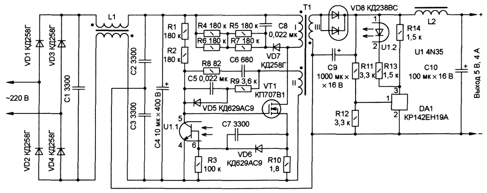
Fig.1. circuit diagram of the device
The device works as follows. After turning on the power supply switching transistor VT1 turns-on and current starts flow by the primary winding of pulse transformer T1. In the winding of feedback transformer II induced EMF, which is the chain of positive feedback - a resistor R9, diode VD5, capacitor C5 comes to the gate field-effect transistor VT1. As a result, developing an avalanche process leading to fully open the switching transistor. It starts with the accumulation of energy in the transformer T1. In the winding of feedback of transformer II EMF is induced, that comes to the gate field-effect transistor VT1 by the chain of positive feedback - a resistor R9, diode VD5, capacitor C5. As a result, an avalanche process develops, that leads to fully opening of the switching transistor. The accumulation of energy starts in the transformer T1. The current increases linearly in the switching transistor VT1, and the voltage with a current sensor resistor R10 through a diode VD6 and capacitor C7 affects on the base of phototransistor optocoupler U1.1, slightly opening it, and as a result, decreases the voltage on the gate of the field-effect transistor. Reverse process starts, that leads to closing of the switching transistor VT1. At this point, a diode VD8 opens and the energy stored in the transformer T1 is transferred to output filter capacitor C9.
When the output voltage for any reason, exceed the nominal value, the stabilizer of DA1 opens, and current begins to flow through it and consistently included optocoupler emitting diode U1.2. Emission of the diode leads to earlier unlocking of optocouplers transistor, and the open state of switching transistor decreases, the energy stored in the transformer is smaller and therefore the output voltage decreases.
If the output voltage decreases, current in the optocouplers emitting diode decreases, and the optocouplers transistor closes. As a result, time of the open state of the switching transistor increases, the energy amount stores more in the transformer and the output voltage restores.
Resistor R3 is required to reduce the influence of the dark current of the optocouplers transistor and improve the thermal stability of the entire device. Capacitor C7 increases the stability of the power source. Circuit C6R8 boost switching processes in transistor VT1 and increases the efficiency of the device.
Dozens of power supplies with output power of 15 ... 25 watts have been made by this scheme.
Instead of the switching transistor VT1 both field and bipolar transistors can be used, for example, series 2T828, 2T839, KT872, KP707, BUZ90, etc. Transistor Optocoupler 4N35 can be replaced by any of the series AOT110, AOT126, AOT128 and stabilizer KR142EN19A - TL431. However, best results were obtained with the imported items (BUZ90, 4N35, TL431).
All resistors in the power supply are for surface-mount, 1206 standard size, power 0,25 W, capacitors C1-C3, C8 - are ceramic with voltage 2kV, C5-C7 - surface mount, standard size 0805, the other ones - any oxide.
Transformer T1 is wound on two stacked together, the annular magnet core K19x11x6,7 of permalloy МП 140. The primary winding contains 180 turns of wire ПЭВ-2 0.35, winding II - 8 turns of wire SEW-2 0.2, winding III at 5V output voltage - 7 turns of the five conductors ПЭВ-2 0.56. Procedure of winding corresponds to their numbering, and the turns of each coil should be evenly distributed around the perimeter of the magnetic circuit.
Inductance coil L1 and L2 are made on the annular magnet core K15x7x6,7 of permalloy МП 140. The first one contains two coils of 30 turns each, wound with wire ПЭВ-2 0.2 at different halves of the magnet core, the second coil is wound with wire ПЭВ-2 0.8 in a single layer over the entire length of the magnet core as will fit.
To reduce the pulsations of output voltage, common point of capacitors C2 and C3 should first be connected to the minus side of the capacitor C10, and then with the other details - the winding III of the transformer T1, minus side of the capacitor C9, resistor R12 and terminal 2 of the stabilizer DA1.
Device assembled on the PCB size 80x60 mm. On one side of the card printed conductors and components for surface mounting are placed, as well as switching transistor VT1 and diode VD8, which are pressed to the aluminum plate - the heat sink of the same size, and on the other - all the rest.
First switching on of the appliance is better to carry by a power supply with current limiting, for example, Б5-50, and the operating voltage should be immediately follows, rather than increase it gradually. Establishment of the device is to tweak the output voltage with divider R11R12 and, if necessary, install with the current sensor R10 of threshold limits the output power (the beginning of a sharp drop in output voltage with increasing load current).
For other output voltage the number of turns of the winding III of the transformer T1 and division ratio of divider R11R12 needed to be proportionaly changed.
Contacts: dytskov@rambler.ru